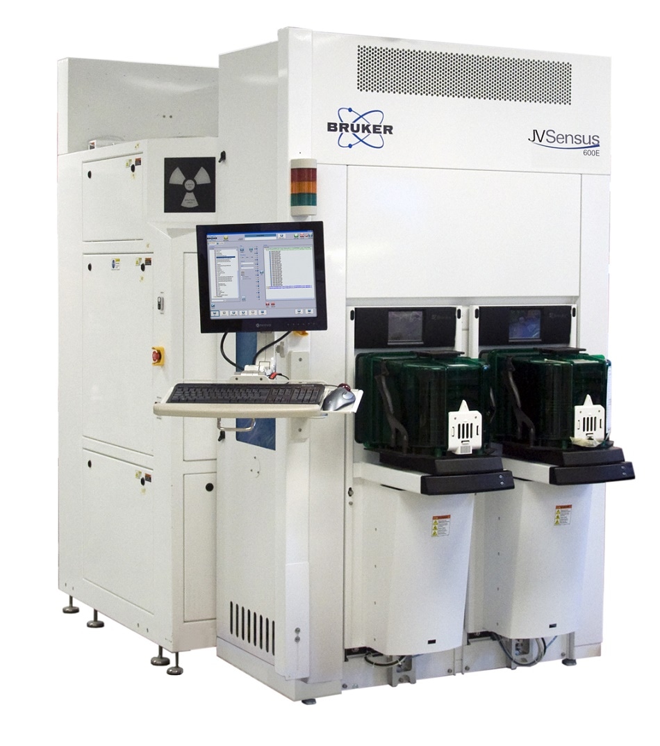
图片来源:布鲁克半导体部门
在2017年Semicon West,Bruker的半导体部门今天宣布,领先的多个半导体制造商已订购JVSENSUS-600E X射线衍射成像系统,用于在线晶粒缺陷监测。JVSENSUS-600E工具配备了高速和高分辨率X射线衍射成像(XRDI)测量能力,可检测和分类由高压力过程引起的广泛的晶体缺陷,例如快速退火和CMP,和CMP,和CMP,和CMP或通过可怜的晶圆处理。JVSENSUS系统允许在退火之前识别出缺陷,这通常是导致晶圆破裂和严重产量损失的关键步骤。通过在过程的早期检测缺陷,半导体制造商可以快速识别导致晶圆损伤并减少产量损失的过程的根本原因。
“We are delighted to have been selected by industry-leading customers to provide defect inspection systems for their production yield improvement,” said David V. Rossi, President of the Bruker Semiconductor Division. “We see these shipments as further validation of the value that early detection of critical defects brings to our customers in reduction of wafer breakage."
As the industry utilizes more aggressive steps within more advanced technology nodes, such as fast annealing strategies, new non-visual defect detection challenges arise. The JVSensus-600E system is capable of detecting a wide range of crystalline defects using X-ray diffraction imaging technique, and is optimised for both blanket and pattern wafers on a single system. This allows a fab to efficiently ramp up processes and quickly identify crystalline defects on product wafers to minimize yield loss from wafer breakage in their production line.
X射线半导体业务副总裁兼总经理Isaac Mazor,Bruker