EV Group (EVG), a leading supplier of wafer bonding and lithography equipment for the MEMS, nanotechnology and semiconductor markets, today announced that the Singapore-MIT Alliance for Research Technology (SMART) has ordered an EVG®850LT fully automated production bonding system designed for silicon-on-insulator (SOI) and direct wafer bonding using low-temp plasma activation processing.
SMART, which is a leading research center established by the Massachusetts Institute of Technology (MIT) in partnership with the National Research Foundation of Singapore, will utilize the EVG850LT system to support its advanced substrate development efforts.
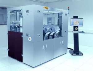 EVG(R)850LT完全自动化的生产键合系统结合了在单个平台中晶片键合的所有基本步骤,以确保在所有阶段确保超清洁的生产过程,从而实现高产,无效的晶圆。它支持各种高级底物,包括在晶格工程基质(SOI)技术(SOI)和硅技术上,直径高达300毫米。(prnewsfoto/ev组)
The MIT research center is located outside the United States in Singapore and has five different research groups, including the Low Energy Electronic Systems (LEES) Research Group, which focuses on integrating silicon CMOS and compound semiconductor materials to enable new integrated circuits (ICs) for wireless devices, power electronics, LEDs, displays and other applications. The LEES Research Group features a state-of-the-art fabrication facility, where the EVG850LT has already been installed and is in use.
根据麻省理工学院材料科学与工程系的尤金·菲茨杰拉德(Eugene Fitzgerald)教授,Smart选择了EVG850LT进行该亚博网站下载中心的高亚博老虎机网登录级研发工作,这是由于该系统的高过程灵活性和性能,EVG在低温结合方面的经验以及在流程开发中的专业知识和支持。“我们的Lees研究小组的宪章是确定新的IC技术,这些技术使能够消耗更少功率的设备,启用更高的性能并为信息系统开放新的应用程序。EVGroup的技术和专业知识将在支持这项工作中发挥重要作用,”菲茨杰拉德教授说。
EVG850平台构建了EVG850LT系统,是唯一旨在在高通量,高收益环境中运行的SOI和直接晶圆粘结平台,将其作为SOI晶圆粘结市场中的行业标准。EVG850LT平台结合了晶圆粘合的所有基本步骤,从清洁和对齐到预键和IR-INSPECTION - 在一个平台中。这样可以确保在所有阶段进行超清洁的生产过程,以实现高产,无效的晶圆,而不是独立的加工单元,而独立的加工单元需要在常规的洁净室环境中手动运输晶片。EVG850支持各种高级底物,包括直径300毫米的晶格工程底物(SOLES)技术上的SOI和硅。
"EVG has been at the forefront of SOI technology development for more than 20 years, and has established a strong expertise and leadership in engineered substrate bonding. We have worked closely with leading research institutes and inventors of SOI technology, and we are very proud that SMART has chosen our high-throughput, high-yield EVG850 system for their advanced technology development efforts," said Frank Huysmans, regional sales director, Asia/Pacific at EV Group. "This is a testament to our leadership in engineered substrates, from R&D to high-volume manufacturing. SOI wafer producers and researchers rely on EVG's equipment to advance the production and technological capabilities of SOI wafers."
关于EV组(EVG)
EV Group (EVG) is a leading supplier of equipment and process solutions for the manufacture of semiconductors, microelectromechanical systems (MEMS), compound semiconductors, power devices and nanotechnology devices. Key products include wafer bonding, thin-wafer processing, lithography/nanoimprint lithography (NIL) and metrology equipment, as well as photoresist coaters, cleaners and inspection systems. Founded in 1980, EV Group services and supports an elaborate network of global customers and partners all over the world.
Source:http://www.evgroup.com