ARenishawinVia Raman microscope has been used in new research that addresses one of the major hindrances to the wider exploitation of graphene: the difficulty in growing large defect-free films.
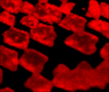
 图像:CVD石墨烯样品的2D石墨烯带宽度的拉曼图。该图像说明了样品区域上石墨烯层的数量的变化,其鲜红色区域由较厚的材料组成,而不是深红色区域。
An international team—led by Oxford University scientists Professor Nicole Grobert and Adrian Murdock— in collaboration with Renishaw plc and researchers from the Forschungszentrum Juelich (Germany) and University of Ioannina (Greece), used a Renishaw inVia Raman microscope to examine film thickness, strain and defects in graphene films.
Graphene is a single layer of carbon atoms and was the first two dimensional material to be discovered. It has very interesting electronic and mechanical properties; it is one of the most conductive materials known to science and has a breaking strength 100 times greater than steel.
通常,当使用化学蒸气沉积(CVD)生长石墨烯时,单个石墨烯薄片与多种不同方向合并,从而产生缺陷。In this work, titled ‘Controlling the Orientation, Edge Geometry and Thickness of Chemical Vapour Deposition Graphene’, and published in the journal ACS Nano, it was found that the orientation of the underlying copper substrate could be used to guide the graphene flakes so they are aligned, and these defects are prevented.
Team member Dr Tim Batten, Raman applications specialist at Renishaw, said, “The inVia Raman spectrometer is a very powerful tool for investigating the properties of graphene. This work gives a much better understanding of CVD graphene growth, which will be important for manufacturing graphene on an industrial scale.”
In 2006 Professor Andrea Ferrari (University of Cambridge), used a Renishaw Raman spectrometer to conduct the first Raman characterisation of graphene. He used samples from its discoverers, Nobel Prize winners Professor Andre Geim and Professor Kostya Novoselov (University of Manchester). Since then, researchers worldwide have used data from Renishaw Raman systems in hundreds of scientific papers on graphene, greatly assisting in the understanding and development of this amazing material.
For further details about the inVia Raman microscope, visitwww.renishaw.com/raman