Introduction最近,由四柱半导体制成的量子点的制造,可以用作量子点激光器和单电子设备的活性层,由于它们在硅(SI)集成电路中的适用性[1-4]引起了很多关注[1-4]。GydF4y2Ba对于这些点的形成,对这些高效率发光装置的密度和大小的控制至关重要。GydF4y2BaIt has been reported that a dot density of 1011GydF4y2Ba厘米GydF4y2Ba-2was achieved using a pregrowth of sub-monolayer carbon [4].在这种情况下,将碳原子掺入Si(001)底物中,并诱导表面应变,导致表面的Si(001)-c(4x4)形成,从而改变了Stranski的锗(GE)生长模式。-Krastanov(SK)模式至Volmer-Weber(VW)模式,导致高密度点形成。GydF4y2Ba表面的点在本实验中随机排列。GydF4y2Ba到目前为止,尚未报道过仅使用自组装技术形成的定期排列点的形成。GydF4y2BaWe have recently found that cubic silicon carbide (3C-SiC)nAnodots were grown with lateral ordering after annealing a c(4x4) surface formed on a Si(001)-2˚off substrate.In this case, it is thought that step bunching occurred during c(4XGydF4y2Ba4)Formation and the alignment of SiC along <110> was achieved due to the effect of the step bunching [5].This surface inducing the SiC dot alignment is expected as a template substrate for the formation of aligned Ge dots. 据报道,由于带隙之间的较大差异,嵌入在SIC层中的GE点有望强烈限制载体[6-8]。GydF4y2Ba但是,在这些研究中,使用了复杂的制造程序,即4H-SIC中的植入,然后进行热退火。GydF4y2BaSo far, the Ge-dot array structure embedded in a 3C-SiC crystal has not been able to be fabricated using simple methods such as chemical vapor deposition (CVD).单甲基类(MMGE)是一种烷基化合物,其分子中含有碳和GE原子。GydF4y2BaIt has been reported that the interaction between carbon and Ge is repulsive on a Si(001) substrate [9-11].因此,预计该源气体将在SI表面分别形成SIC点和GE点,并被认为适合形成嵌入在SIC中的纳米点等纳米结构。GydF4y2Ba为了确认这一事实,重要的是要了解MMGE和SI(001)底物之间的反应过程。GydF4y2BaIn this study, we investigated the surface reaction of MMGe using reflection high-energy electron diffraction (RHEED) and X-ray photoelectron spectroscopy (XPS).之后,我们还尝试形成嵌入SIC层中的GE点,并通过光致发光(PL)测量分析其光学特性。GydF4y2Ba 实验细节GydF4y2Ba从N型Si(001)晶片切割的Si底物(ρ)GydF4y2Ba< 0.02使用ωCM)。GydF4y2BaThe substrates were cleaned using an organic solvent in an ultrasonic bath followed by dipping them into H2GydF4y2Ba所以GydF4y2Ba4GydF4y2Ba+ H2GydF4y2BaoGydF4y2Ba2GydF4y2Bam我Xtures.After rinsing in deionized water, they were fixed on a sample holder made of molybdenum (Mo) and were loaded into a load-lock chamber.撤离后,它们被转移到反应室中。GydF4y2Ba然后si(001)-2GydF4y2BaXGydF4y2Ba通过在600°C的600°C下预击10小时,制备1条干净的表面,然后在反应室的超高真空(UHV)下闪烁至1250°C大约5 s。GydF4y2BaSubstrates were heated by DC current flow and substrate temperatures were measured using an optical pyrometer, which was calibrated using a chromel-alumel thermocouple. 形成2之后GydF4y2BaXGydF4y2Ba1CleAnsurfaces, the substrates were set at a moderate temperature between 400 and 800˚C prior to MMGe supply.在反应期间的MMGE气压设置为1.0GydF4y2BaXGydF4y2Ba10-6Torr.During the reaction, a change in surface structure was observed in situ by RHEED at an accelerating voltage of 30 kV.使用数字摄像机记录荧光屏幕上的衍射图案,以评估Rheed强度和晶格常数的变化(也是表面重建的周期距离)。GydF4y2BaThe changes in RHEED intensity were analyzed using a personal computer.另一方面,晶格常数通过衍射几何形状的关系1/d = r/(λl)评估。GydF4y2BaHere, d is the lattice constant of the sample surface and r is the lateral distance between the specular spot and the spot corresponding to d on the fluorescent screen.That is, r is the distance from the central rod indicated in Figure 2.λ and L are the wavelength of the electron beam and the camera length, respectively, which are characteristic dimensions of the experimental apparatus.λL was evaluated using the periodic distance corresponding to the Si bulk spot (d=0.384nm).反应后,将样品转移到分析室,并通过STM观察到表面结构。GydF4y2BaThe composition of the surface layer was analyzed ex situ by XPS.为了执行PL测量,制造了两种类型的结构。GydF4y2Ba第一个是在SI(001)上提供的MMGE形成的。GydF4y2Ba第二个是由在SI(001)上提供SIC点的MMGE形成的。GydF4y2Ba两者都用SIC层盖,该层在MMGE反应后使用单甲基硅烷(MMS)在700°C下生长。GydF4y2Ba使用LD(λ::GydF4y2Ba785nm, 300 mW) at 77K. 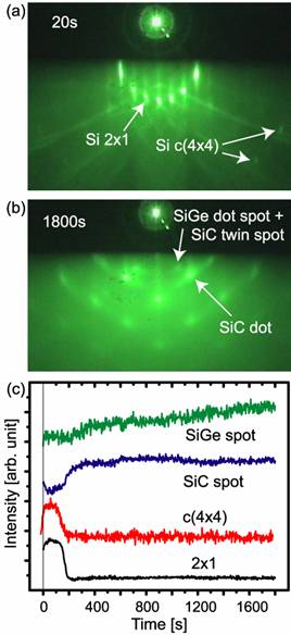
图1。GydF4y2BaRHEED pattern after exposure of MMGe on Si(001) for (a) 20s and (b) 1800s. (c) Change in RHEED intensity for each spot. Results and DiscussionRHEED Observation of Surface Reaction在低于600的底物温度下,几乎没有观察到Si和MMGE之间的表面反应GydF4y2Ba°C。GydF4y2Ba从这些样品的STM测量值中,除了在这些生长条件下仅吸附的分子或极小的簇外,在表面上没有观察到显着的特征。GydF4y2BaAt substrate temperatures of 600 to 800°C, diffraction spots derived from c(4XGydF4y2Ba4)structures appeared, followed by the appearance of SiC and other spots,在MMS反应中未观察到。GydF4y2BaFigure 1 shows the RHEED patterns after (a) 20 s and (b) 1800 s supplies of MMGe at 700°C(c)Rheed强度的变化。GydF4y2Ba从这个图中发现,在C之后出现了SIC斑点(4GydF4y2BaXGydF4y2Ba4)structures disappeared, which was similar to the use of the reaction between MMS and Si(001).The hazy spots labeled “SiGe dot spot + SiC twin spot”, which were not observed in the MMS case under the same experimental conditions [12], appeared in the case of MMGe. 假设结构域的晶体结构是新衍射斑的起源,是锌蓝的结构,估计晶体的晶格常数估计为0.66 nm,大于块状GE(0.566 nm)。GydF4y2Ba据报道,SIC双胞胎结构是在SIC生长的初始阶段形成的,碳原子过多(以–CH的形式形式GydF4y2Ba3GydF4y2Ba)on the surface [13].In the MMGe case, this source gas can be decomposed more easily than MMS due to the weak bond strength of Ge-C [14]. 因此,据推测,在初始阶段存在过量的碳原子下形成了SIC双胞胎结构。GydF4y2Ba为了确认该点是否包含来自GE的点的贡献,使用高压供应MMGE制备了厚的GE层。GydF4y2BaThe description “Ge-containing dots” means that both Ge and SiGe dots can exist on the surface due to the possibility of intermixing between Ge from MMGe molecules and Si from Si substrate in the presence of hydrogen atoms on the surface [15].在本文中,我们将“含Ge的点”描述为Rheed模式中的SIGE。GydF4y2BaFigure 2 shows RHEED patterns obtained from (a)a 2XGydF4y2Ba1表面,(b)MMGE在2上暴露后的表面GydF4y2BaXGydF4y2Ba700处的1个表面GydF4y2Ba°CFor 5400 s, and (c) the surface after high-pressure growth (~10-2在同一底物温度下的表面上的托尔)在2 s。GydF4y2Ba从图2(c)中,将晶格常数评估为0.57nm,与GE散装相吻合,并且比SIC Twin Spot(0.66 nm)小。GydF4y2BaIt was thought that this small deviation of the lattice constant (0.57 nm) from the literature value (0.566 nm) was due to the occurrence of stress relaxation in the Ge layer.这些结果表明,随着层厚度的增加,表面组成在GE中变得更丰富,最后形成了GE层,其具有类似于GE Bumb的晶格常数。从这些结果中可以认为,图1(a)中标记为“ Sige Dot Spot + SIC Twin斑点”的斑点包含来自GE的DOT和SIC TWIN结构的贡献,这是MMGE和SI之间的反应的初始阶段(001))。GydF4y2Ba 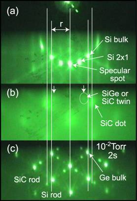
图2。GydF4y2BaRHEED patterns of (a)2x1 surface (b)surface after MMGe exposure for 5400s and (c)surface after high-pressure exposure of MMGe.圆表示GE(SIGE) + SIC双斑。GydF4y2Ba Analys是表面成分GydF4y2Ba图3显示了在700°C和高压生长后用MMGE生长的样品的SI2P和GE3D成分的典型XPS光谱。GydF4y2Ba在图3(a)中,将SI2P峰分成2个峰:Si-Si和Si-C。GydF4y2BaThe Si-Ge bond could not be distinguished from the Si-Si bond due to the similarity of their electronegativity (Si:1.8, Ge:2.0).In the Ge3d spectrum, on the other hand, a peak originating from the Ge-Ge or Ge-Si bond was detected at 29.0 eV.这表明,即使该样品的键的主要成分尚不清楚,也存在于表面上的GE。GydF4y2Ba高压生长后,Si-C和Si-Si键的峰完全从SI2P频谱中完全消失(图3(c)),在GE3D频谱中仅观察到GE-GE键(未显示)。GydF4y2BaThis result indicates that the surface was covered with a Ge layer after high-pressure growth.人们认为,由于基板缺乏SI供应,因此表面组成在高压生长后变得更丰富,并最终成为GE层。GydF4y2Ba该结果与Rheed获得的结果非常吻合。GydF4y2Ba也就是说,SIGE + SIC双斑的强度不断增加,而SIC生长停止。GydF4y2Ba从这些结果中可以认为,在初始反应阶段,在Si(001)表面共存的含GE的点和SIC纳米植物,然后是GE层的生长。GydF4y2Ba 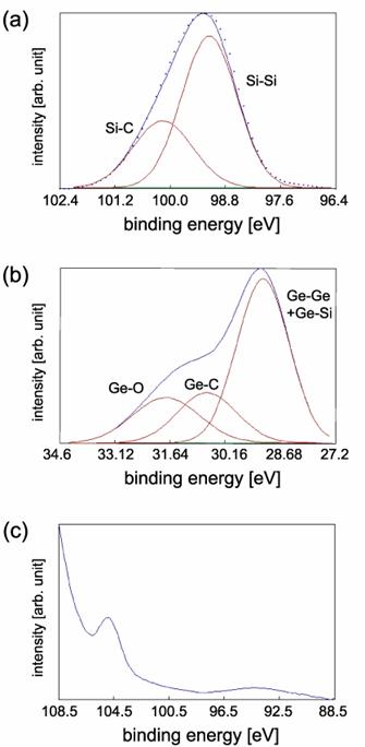
图3。GydF4y2BaMMGE暴露后获得的XPS光谱。GydF4y2Ba(a)Si2p,(b)GE3D和(C)高压暴露后的SI2P光谱。GydF4y2Ba CHAracterization of Optical Property
Figures 4(a) and (b) show the PL spectra obtained from the Ge embedded in SiC on a Si substrate without SiC dots on Si(001) and with SiC dots, respectively.In both spectra, weak peaks at 0.84 eV and 0.95 eV were observed.尽管这些峰的起源尚不清楚,但据报道,在3.65 mL GE沉积在Si(001)底物上,在0.85 eV处观察到来自GE的PL峰(NP发光),其含量为0.2 ml c [16]。GydF4y2BaFrom an experiment of Ge deposition on Si(001), TO and NP luminescences from a Ge wetting layer of在0.94 eV和0.99 eV下观察到3.9 mL [17]。GydF4y2Ba从这些结果中可以推测出图4中所示的峰可能对应于GE点和GE润湿层(我们实验中的大GE点)。GydF4y2Ba但是,在这项研究中,SIGydF4y2Ba1-xCGydF4y2BaXGydF4y2BaC的合金层(4GydF4y2BaXGydF4y2Ba4)在表面形成形成和SIC盖层。GydF4y2Ba因此,还认为从表面应变和不同组合物中对GE点的贡献。GydF4y2BaThe slight shift of the peak at 0.95 eV shown in Figure 4(b) may be due to the strain caused by SiC dots.目前,图4中所示的峰的起源尚不清楚,因为PL峰被认为受许多参数(例如应变)的影响。GydF4y2Ba然而,据推测,由于峰位置与文献中报道的峰[16,17],图4中所示的峰与GE有关。GydF4y2BaFurther investigation is required to determine the origin of the emissions。GydF4y2Ba 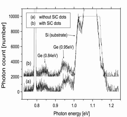
Figure 4.PL spectra of Ge embedded in SiC structure. Ge dots were formed (a) without SiC dots layer and (b) on SiC dot layer. 结论GydF4y2BaIn this study, we have analyzed the structural evolution of a Si(001) surface and the change in surface composition during a reaction of MMGe on the surface.发现一个C(4GydF4y2BaXGydF4y2Ba4)structure formed before SiC nucleation similarly to the MMS case, and both SiC dots and Ge-related dots formed separately on the surface.The growth of SiC dots and Ge-containing dots stopped due to the lack of Si out diffusion from the Si substrate (intermixing in the case of Ge) after the formation of SiC and Ge on the entire surface area.随着与Si基板和点之间的距离的距离增加,含GE的点的组成变得更加丰富。GydF4y2Ba用SIC限制GE点后,在约0.84 eV和0.95 eV处观察到弱PL信号。GydF4y2Ba这些峰被认为来自GE点和GE润湿层。GydF4y2Ba References1。GydF4y2BaO.Leifeld,A。Beyer,E.Müller,D.Grützmacher和K.GydF4y2BaKern, “Nucleation of Ge问GydF4y2BaUantumGydF4y2BadGydF4y2BaC合金SI(001)上的OTGydF4y2BasGydF4y2BaUrface”,薄膜,380(2000)176-179。GydF4y2Ba 2。GydF4y2BaJ. Y. Kim,S。H。Ihm,J。H。Seok,C。H。Lee,E。–K。Suh和H. J. Lee,“成长GydF4y2BatGydF4y2BaemperaturedGydF4y2Baexpentence on theGydF4y2BaFGydF4y2Ba的GydF4y2BaCGydF4y2BaArbon诱导的GEGydF4y2Ba问GydF4y2BaUantumGydF4y2BadGydF4y2BaOT”,薄膜,369(2000)96-99。GydF4y2Ba 3。GydF4y2BaY. Wakayama,G。Gerth,P。Werner和L. V. Sokolov,“效果GydF4y2BasGydF4y2BaUbmonolayerGydF4y2BaCGydF4y2BaArbon OnGydF4y2BanGydF4y2BaAnoscale GedGydF4y2BaotGGydF4y2Basi(001)上的rowthGydF4y2BasGydF4y2BaUbstrates”,冲浪。Sci。,493(2001)399-404。GydF4y2Ba 4。GydF4y2BaM. Stoffel,L。Simon,J。L。Bischoff,D。Aubel,L。Kubler和G. Castelein,“ GEGydF4y2BaGGydF4y2BarowthmGydF4y2Ba颂GydF4y2BamGydF4y2BaODIFIENGGydF4y2BaCGydF4y2BaArbon诱导的Si(001)-c(4×4)表面”,薄膜,380(2000)32-35。GydF4y2Ba 5。GydF4y2BaM. Harashima,K。Yasui,M。Takata和T. Akahane,“ SI(001)-C(4x4)GydF4y2BaAGydF4y2Ba纳尔分析GydF4y2BatGydF4y2Ba哇GydF4y2BaFGydF4y2Ba工业GydF4y2BatGydF4y2BaimplateGydF4y2BasGydF4y2Baubstrate fornGydF4y2BaAno-dot”, International Journal of Mechanical and Materials Engineering, 1 (2006) 12-17. 6。GydF4y2BaK. Ait-Mansour,D。Dentel,J。L。Bischoff,L。Kubler,M。Diani,A。Barski,M。Derivaz和P. Noe,“ GEGydF4y2Ba问GydF4y2BaUantumGydF4y2BadGydF4y2BaOTSGydF4y2BalGydF4y2BaArgeGydF4y2BabGydF4y2BaAndGydF4y2BaGGydF4y2BaAPGydF4y2BasGydF4y2Baemiconductor:GydF4y2BaFGydF4y2Ba我rstGGydF4y2BarowthsGydF4y2Ba4H-SIC(0001)上的tages”,Physica,E 23(2004)428-434。GydF4y2Ba 7。GydF4y2Bach。舒伯特(W.GydF4y2BaGGydF4y2Baroup IVnGydF4y2BaSIC中的AnocrystalsGydF4y2Ba我GydF4y2BaonbGydF4y2BaeAmGydF4y2BapGydF4y2Barocessing”, NIM B, 191 (2002) 428-432. 8。GydF4y2BaH. –CH。Weissker,J。Furthmuller和F. Bechstedt,“光学GydF4y2BapGydF4y2BaGE和SI的RopertiesGydF4y2BanGydF4y2BaAB的肛门晶体GydF4y2Ba我GydF4y2BaNitioGydF4y2BaCGydF4y2BaAlCulations. I. EmbeddednGydF4y2BaAnocrystallites”, Phys. Rev. B, 65 (2002) 155327. 9。GydF4y2BaA. Sakai,Y。Torige,M。Okada,H。Ikeda和Y. Yasuda,“原子GydF4y2BaeGydF4y2Basi的波动GydF4y2Ba1-x-yGEGydF4y2BaXGydF4y2BaCGydF4y2BayGydF4y2BatGydF4y2BaH我nGydF4y2BaFGydF4y2Ba我lmson Si(001)sGydF4y2Baurfaces”, Appl. Phys. Lett., 79 (2001) 3242-3244. 10.H. Jacobsson,J。Xiang,N。Herbots,S。Whaley,P。Ye和S. Hearne,J。Appl。物理。81(1997)3081。GydF4y2Ba 11。GydF4y2BaP. C. Kelires, “Monte Carlo Studies of Ternary Semiconductor Alloys: Application to the Si1-x-yGEGydF4y2BaXGydF4y2BaCGydF4y2BayGydF4y2Ba系统”,物理。Rev. Lett。,75(1995)1114-1117。GydF4y2Ba 12。GydF4y2BaY. Narita, T. Inubushi, M. Harashima, K. Yasui, and T. Akahane, “InitialsGydF4y2BatAGeof 3C–SiCGGydF4y2Basi(001)上的rowth–2×1sGydF4y2Baurface usingmGydF4y2Baonomethylsilane”, Appl. Surf. Sci., 216 (2003) pp.575-579. 13。GydF4y2BaM. Kitabatake and J. E. Green, “Surface-Structure-Controlled Heteroepitaxial Growth of 3C-SiC3x2 on Si(001): Simulations and Experiments”, Jpn. J. Appl. Phys., 35 (1996) 5261-5273. 14。GydF4y2BaT. Akane,M。Sano,H。Okumura,Y。Tubo,“特征GydF4y2BaGGydF4y2Ba作为源GydF4y2BamGydF4y2Ba卵巢GydF4y2BabGydF4y2BaeAmGydF4y2BaeGydF4y2BaPutaxialGydF4y2BaGGydF4y2BarowthGydF4y2BasGydF4y2Batrain-compensated Si1-x-yGEGydF4y2BaXGydF4y2BaCGydF4y2BayGydF4y2BaSi(001)HGydF4y2BaEterostructure”,J。CrystalGrowth,203(1999)80-86。GydF4y2Ba 15。GydF4y2BaT. Murata and M. Suemitsu, “GeH4GydF4y2BaAdsorption on Si(001) at RT: transfer of HAGydF4y2BaToms到SIGydF4y2BasGydF4y2Ba我tesAndGydF4y2BaAGydF4y2BatomiceGydF4y2BaXCHAnGebetween Si and Ge”, Appl. Surf. Sci., 224 (2004) 179-182. 16。GydF4y2BaO. G. Schmidt,C。Lange,K。Eberl,O。Kienzle和F. Ernst,“GydF4y2BapGydF4y2Bare-grownCGydF4y2BaArbon OntHeGydF4y2BaFGydF4y2Ba的GydF4y2BaGGydF4y2BaermaniumdGydF4y2BaOT”,薄膜,321(1998)70-75。GydF4y2Ba 17。GydF4y2BaH. Sunamura,N。Usami,Y。Shiraki和S. Fukatsu,“岛屿GydF4y2BaFGydF4y2Ba在期间GydF4y2BaGGydF4y2BaSi(100)上GE的Rowth:aGydF4y2BasGydF4y2Batudy使用GydF4y2BapGydF4y2Ba热发光GydF4y2BasGydF4y2Ba胸腔镜检查”,应用。物理。Lett。,66(1995)3024-3026。GydF4y2Ba ContactDetails
Masayuki Harashima Department of Electrical Engineering, Faculty of Engineering
纳戈卡技术大学GydF4y2Ba
1603-1 kamitomioka-cho,nagaokaGydF4y2Ba
Niigata 940-2188GydF4y2Ba
Japan Email:[电子邮件保护]GydF4y2Ba |
Ariyuki Kato Department of Electrical Engineering, Faculty of Engineering
纳戈卡技术大学GydF4y2Ba
1603-1 kamitomioka-cho,nagaokaGydF4y2Ba
Niigata 940-2188GydF4y2Ba
Japan |
汉字YasuiGydF4y2Ba Department of Electrical Engineering, Faculty of Engineering
纳戈卡技术大学GydF4y2Ba
1603-1 kamitomioka-cho,nagaokaGydF4y2Ba
Niigata 940-2188GydF4y2Ba
Japan
|
塔达西·阿卡哈恩(Tadashi Akahane)GydF4y2Ba Department of Electrical Engineering, Faculty of Engineering
纳戈卡技术大学GydF4y2Ba
1603-1 kamitomioka-cho,nagaokaGydF4y2Ba
Niigata 940-2188GydF4y2Ba
Japan
|
高田MasasukeGydF4y2Ba Department of Electrical Engineering, Faculty of Engineering
纳戈卡技术大学GydF4y2Ba
1603-1 kamitomioka-cho,nagaokaGydF4y2Ba
Niigata 940-2188GydF4y2Ba
Japan |
|
|